 |
| December 21, 2021 | Volume 17 Issue 47 |
Designfax weekly eMagazine

Archives
Partners
Manufacturing Center
Product Spotlight
Modern Applications News
Metalworking Ideas For
Today's Job Shops
Tooling and Production
Strategies for large
metalworking plants
Semiconductor breakthrough from IBM and Samsung upends conventional design
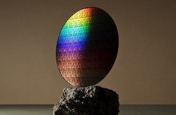
It's Moore's Law, Schmoore's Law at IBM's Albany Nanotech Complex, where a joint effort between Big Blue and Samsung has rewritten the rules for semiconductor design -- creating a new vertical transistor architecture with 85% energy savings and the allure of smartphones that get charged once a week.
Moore's Law, the principle that the number of transistors incorporated in a densely populated IC chip will approximately double every two years, is quickly nearing what are considered insurmountable barriers. Simply put, as more and more transistors are crammed into a finite area, engineers are running out of space.
Historically, transistors have been built to lie flat upon the surface of a semiconductor, with the electric current flowing laterally, or side-to-side, through them. With new Vertical Transport Field Effect Transistors, or VTFET, IBM and Samsung have successfully implemented transistors that are built perpendicular to the surface of the chip with a vertical, or up-and-down, current flow.
IBM says the VTFET design addresses many barriers to performance and limitations to extend Moore's Law as chip designers attempt to pack more transistors into a fixed space. It also influences the contact points for the transistors, allowing for greater current flow with less wasted energy. Overall, the new design aims to deliver a two times improvement in performance or an 85% reduction in energy use as compared to scaled finFET alternatives.
Recently, IBM announced a 2-nm chip technology breakthrough which will allow a chip to fit up to 50 billion transistors in a space the size of a fingernail. VTFET innovation focuses on a whole new dimension, which offers a pathway to the continuation of Moore's Law.
The new vertical transistor engineering could help the semiconductor industry continue its relentless journey to deliver significant improvements. IBM is pretty heady in its forecasts, but the company sees a near-ish future that includes:
- Smartphone batteries that could go over a week without being charged, instead of days.
- A potential device architecture that enables semiconductor device scaling to continue beyond the nanosheet state-of-the-art tech of today.
- Energy-intensive processes, such as cryptomining operations and data encryption, could require significantly less energy and have a smaller carbon footprint.
- Continued expansion of Internet of Things (IoT) and edge devices with lower energy needs, allowing them to operate in more diverse environments like ocean buoys, autonomous vehicles, and spacecraft.
Innovation at the Albany complex in New York is often directed toward commercialization, and on that end of the chip lifecycle today the companies also announced that Samsung will manufacture IBM's chips at the 5-nm node. These chips are anticipated to be used in IBM's own server platforms. This follows the announcement in 2018 that Samsung would manufacture IBM's 7-nm chips, which became available in the IBM Power10 family of servers earlier this year. The IBM Telum processor, also revealed earlier this year, is similarly manufactured by Samsung using IBM's designs.
Source: IBM
Published December 2021
Rate this article
View our terms of use and privacy policy